Ablation of thin layers for the electronics sector
The electronics and semiconductors sector is already well accustomed to lasers, but the technology is developing and new applications are appearing, especially regarding the ablation of thin layers.
High speed production rates
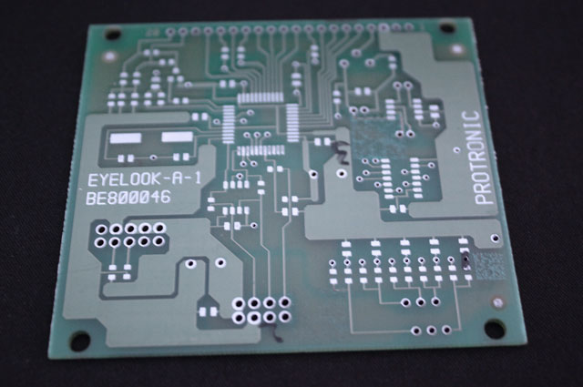
Currently marking and cutting are quite widespread regarding the processing and machining of metals, plastics and silicon. To that is added the selective machining and ablation of thin layers, all at a high speed where reproducibility is the key.
Laser on increasingly large surfaces
We also encounter electronic circuits on increasingly large surfaces where LASEA is specialised in providing reproducible solutions, with high precision (of the order of tens of microns) on increasingly large surfaces (photovoltaic, lighting, surface texturing, etc).